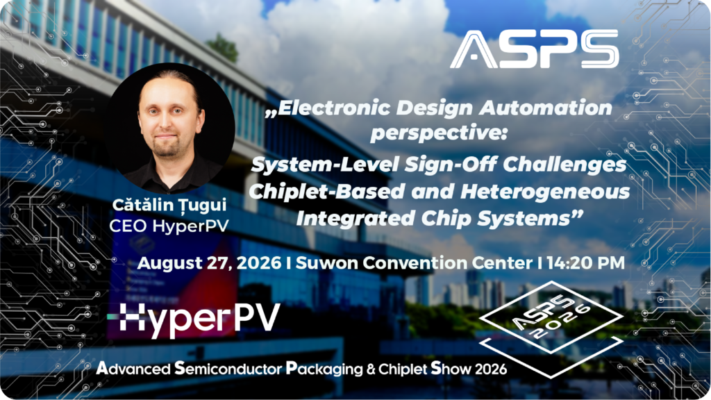
The South Korea, Suwon City —August 26-28, 2026— HyperPV, a deep tech IC Verification startup, had the privilege of participating in the Advanced Semiconductor Packaging & Chiplet Show (ASPS) —an event that brought together leading companies, researchers, technology providers, and industry experts from across the semiconductor ecosystem to discuss the technologies shaping the next generation of integrated systems, including 2.5D and 3D-IC architectures, chiplets, advanced substrates and interconnects, heterogeneous integration, and next-generation semiconductor packaging.
HyperPV was proudly represented at the Advanced Semiconductor Packaging & Chiplet Show (ASPS) 2026 by our CEO, Catalin Adrian Tugui, and VP of Business Development, Anca Marcu, bringing HyperPV’s perspective on the growing verification challenges created by advanced packaging, chiplet-based architectures, and heterogeneous integration.
During ASPS 2026, HyperPV engaged in valuable discussions around system-level physical verification, advanced packaging sign-off, multi-die integration, interoperability, and the rapidly increasing complexity and scale of modern semiconductor systems.
On August 27, a key highlight of HyperPV’s participation was the KPIA seminar, where our CEO, Catalin Adrian Tugui, delivered the presentation:
“EDA (Electronic Design Automation) Perspective: System-Level Sign-Off Challenges for Chiplet-Based and Heterogeneous Integrated Chip Systems.”
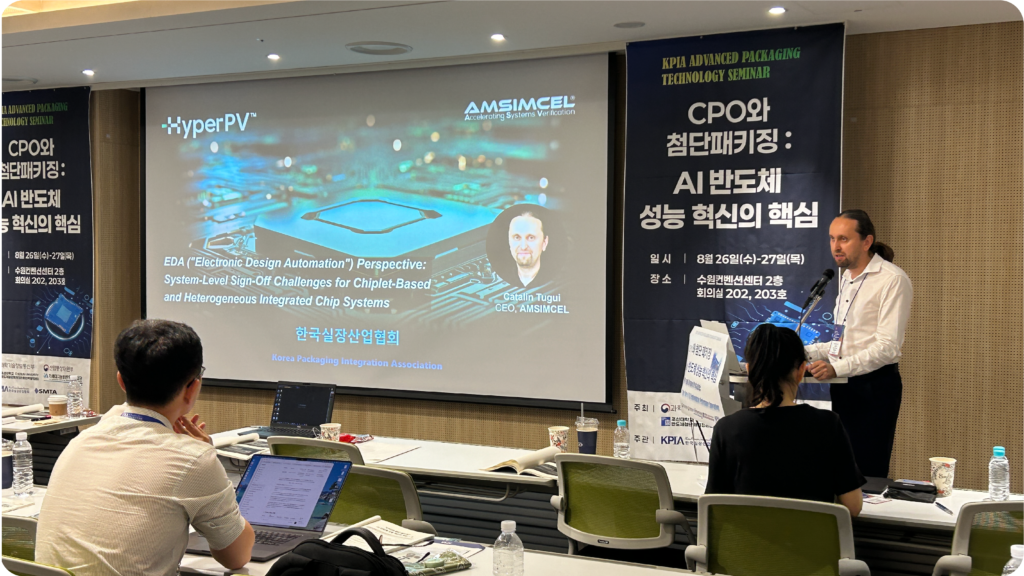
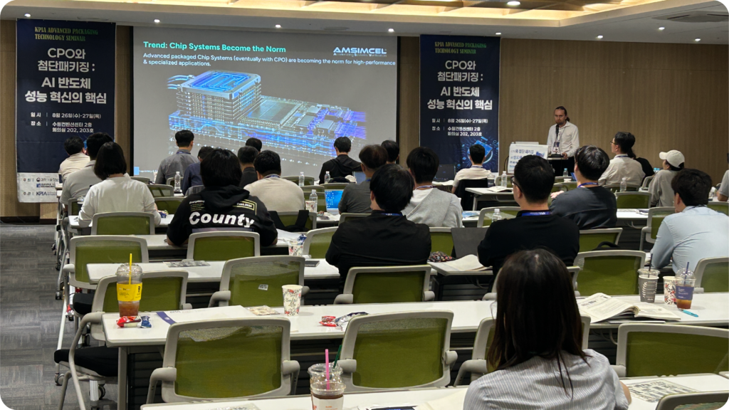
The presentation explored how the transition from traditional monolithic ICs toward increasingly complex heterogeneous systems is creating a new class of challenges for Electronic Design Automation.
These challenges extend beyond the verification of individual dies and increasingly require full-system sign-off across chiplets, interposers, packages, interfaces, power delivery structures, and other active and passive components.
Particular attention was given to three fundamental challenges shaping the future of EDA:
- Architecture heterogeneity – combining different process nodes, technologies, chiplets, memories, interposers, substrates, and package components within the same system.
- System capacity and complexity – as advanced systems move toward hundreds of billions and eventually more than one trillion transistors at system level.
- Standards and interoperability – enabling reliable integration and verification across different foundries, OSATs, chiplet providers, packaging technologies, and EDA environments.
The discussions at ASPS reinforced the need for verification methodologies capable of moving beyond die-level analysis toward a true system-level sign-off framework for heterogeneous integrated systems.
“Our participation at ASPS 2026 is an important opportunity to engage with the advanced packaging and chiplet ecosystem. As semiconductor architectures evolve from individual dies toward increasingly complex heterogeneous systems, physical verification must evolve with them. The industry needs scalable technologies capable of verifying not only individual components, but the complete integrated system.,” said Catalin Tugui, CEO of HyperPV.
At HyperPV, we are developing the next generation of GPU-accelerated Physical Verification solutions for advanced packaging and heterogeneous integrated systems, addressing the growing capacity, performance, and interoperability challenges associated with increasingly complex chiplet-based, 2.5D, and 3D-IC architectures.
ASPS 2026 also provided a valuable platform to exchange ideas with semiconductor manufacturers, packaging specialists, OSATs, EDA companies, research organizations, and technology partners, while exploring new opportunities for collaboration across the global semiconductor ecosystem.
As HyperPV continues to expand its activities in advanced semiconductor verification, we remain focused on developing technologies capable of enabling faster, scalable, and reliable system-level sign-off for the next generation of integrated chip systems.
About the Advanced Semiconductor Packaging & Chiplet Show (ASPS)
The Advanced Semiconductor Packaging & Chiplet Show (ASPS) is an international semiconductor industry event focused on the rapidly evolving fields of advanced packaging, chiplets, heterogeneous integration, and next-generation semiconductor technologies.
The event brings together companies and experts from across the semiconductor value chain, including foundries, OSATs, equipment and materials suppliers, EDA companies, research institutions, system companies, and semiconductor technology developers.
ASPS provides a platform for the industry to explore new packaging architectures, integration technologies, manufacturing approaches, standards, and design methodologies required to support increasingly complex 2.5D, 3D-IC, and chiplet-based systems. For more information please visit the page https://www.semipkgshow.com.


